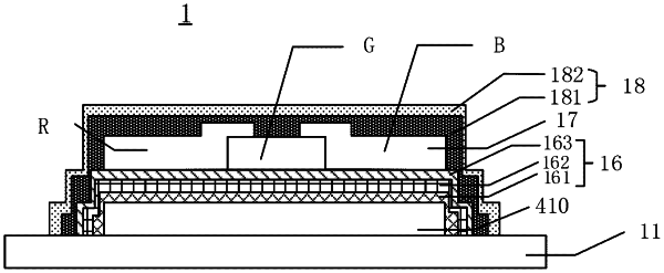
| CPC H10K 59/8722 (2023.02) [H10K 59/1201 (2023.02); H10K 59/38 (2023.02); H10K 59/873 (2023.02)] | 17 Claims |

|
1. A display device, comprising:
an array substrate and a first thin film encapsulation layer disposed on the array substrate,
wherein the array substrate is a silicon based organic light-emitting diode array substrate, and the array substrate comprises:
a silicon substrate and a light-emitting device disposed on the silicon substrate;
a second thin film encapsulation layer disposed between the light-emitting device and the first thin film encapsulation layer;
a color filter layer disposed between the first thin film encapsulation layer and the second thin film encapsulation layer,
wherein at each edge of the first thin film encapsulation layer, an orthographic projection of the array substrate on a plane parallel to the array substrate extends beyond an orthographic projection of the first thin film encapsulation layer on the plane;
a cover panel covering the first thin film encapsulation layer; and
a sealant disposed at sides of a periphery of the cover panel and connecting the cover panel with the array substrate,
wherein an adhesive height of the sealant at the sides of the periphery of the cover panel is larger than ½ of a thickness of the cover panel and less than the thickness of the cover panel.
|