| CPC H10K 59/65 (2023.02) [G09G 3/3266 (2013.01); H10K 59/1213 (2023.02); H10K 59/131 (2023.02)] | 13 Claims |

|
1. A display apparatus comprising:
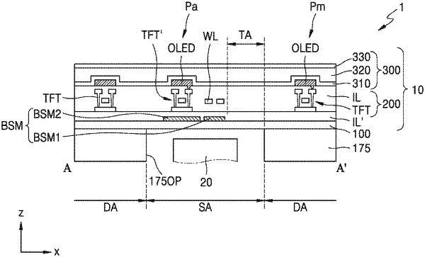
a substrate having a display area, and a sensor area comprising a transmission portion;
a bottom metal layer on the sensor area, and defining an opening corresponding to the transmission portion;
a thin film transistor on the bottom metal layer, and comprising a semiconductor layer and a gate electrode on the semiconductor layer; and
an organic light-emitting diode electrically connected to the thin film transistor, and comprising a pixel electrode, an organic emission layer, and an opposite electrode,
wherein the bottom metal layer fully overlaps an emission area of the organic light-emitting diode, and
wherein a resolution of an image provided by the sensor area is less than a resolution of an image provided by the display area.
|