| CPC H10K 59/353 (2023.02) [H10K 59/122 (2023.02); H10K 59/123 (2023.02); H10K 59/124 (2023.02); H10K 59/352 (2023.02)] | 20 Claims |

|
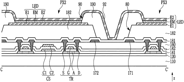
1. A display device, comprising:
a substrate;
a transistor disposed on the substrate and including a semiconductor layer, a gate electrode disposed on the semiconductor layer, and source and drain electrodes, disposed on the gate electrode;
a gate insulating, layer disposed between the semiconductor layer and the gate electrode;
an interlayer insulating aver dispose between the gate electrode and the source and drain electrodes;
a first insulating layer disposed on at least one of a top s dace of the source electrode of the transistor and a top surface of the drain electrode of the transistor;
a second insulating layer disposed between at least one of the top surface of the source electrode of the transistor and the top surface of the drain electrode of the transistor and the first insulating layer;
a third insulating layer disposed on the first insulating layer; and
a first pixel electrode and a second pixel electrode disposed on the first insulating layer to be adjacent to each other, wherein
the first insulating layer includes a first opening disposed between the first pixel electrode and the second pixel electrode,
the second insulating layer includes a portion completely overlapping the first opening,
the third insulating layer includes a portion that directly contacts the second insulating layer, and
the third insulating layer includes a groove or an opening that overlaps the first opening in a thickness direction of the substrate.
|