| CPC H10K 59/131 (2023.02) [H10K 59/1213 (2023.02); H10K 59/1216 (2023.02)] | 14 Claims |

|
1. A display panel comprising:
a substrate;
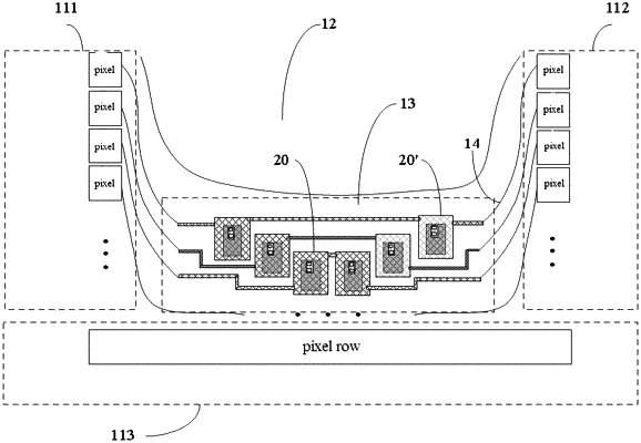
a display area and a notch area on the substrate, wherein the display area at least partially surrounds the notch area; and
a capacitance compensation area, wherein the capacitance compensation area is located on a side of the display area facing the notch area,
wherein the capacitance compensation area comprises a plurality of capacitance compensation units, and each capacitance compensation unit of at least some of the plurality of capacitance compensation units comprises:
a first conductive layer, wherein the first conductive layer is electrically connected to one of a plurality of gate lines;
a second conductive layer, wherein an orthographic projection of the second conductive layer on the substrate at least partially overlaps with an orthographic projection of the first conductive layer on the substrate; and
a first insulating layer between the first conductive layer and the second conductive layer, wherein the first insulating layer is configured to electrically insulate the first conductive layer from the second conductive layer,
wherein the second conductive layer is located on a side of the first conductive layer away from the substrate, and each capacitance compensation unit further comprises:
a second insulating layer, wherein the second insulating layer is located on a side of the second conductive layer away from the first conductive layer; and
a fifth conductive layer, wherein the fifth conductive layer is located on a side of the second insulating layer away from the first conductive layer;
wherein a first via-hole structure is provided in the second insulating layer, and the fifth conductive layer is electrically connected to the second conductive layer through the first via-hole structure;
wherein each capacitance compensation unit further comprises:
a third insulating layer, wherein the third insulating layer is located on a side of the fifth conductive layer away from the substrate; and
a first electrode layer, wherein the first electrode layer is located on a side of the third insulating layer away from the substrate, and the first electrode layer is electrically connected to a DC signal; and
wherein a second via-hole structure is provided in the third insulating layer, and the first electrode layer is electrically connected to the fifth conductive layer through the second via-hole structure.
|