| CPC H10K 59/131 (2023.02) [H10K 50/8426 (2023.02); H10K 59/1213 (2023.02); H10K 59/122 (2023.02); H10K 59/126 (2023.02); H10K 59/18 (2023.02)] | 18 Claims |
|
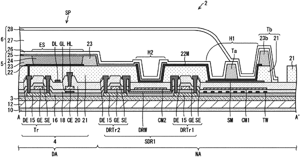
1. A display device comprising:
a display area including a plurality of subpixels each including a subpixel circuit including a transistor; and
a non-display area located in a periphery of the display area, where the plurality of subpixels is not formed,
wherein in the display area,
a first metal layer, including an electrode at a lower layer, is included in the subpixel circuit,
a first inorganic insulating film is formed at an upper layer of the first metal layer,
a second metal layer is formed at an upper layer of the first inorganic insulating film and includes an electrode, among electrodes included in the subpixel circuit,
a second inorganic insulating film is formed at an upper layer of the second metal layer,
a third metal layer is formed at an upper layer of the second inorganic insulating film and includes an electrode, among the electrodes included in the subpixel circuit,
a flattening film is formed at an upper layer of the third metal layer, and
a light-emitting element is formed at an upper layer of the flattening film and includes a first electrode and a second electrode with a light-emitting layer interposed between the first electrode and the second electrode,
the first electrode is formed in an island shape for each of the plurality of subpixels,
the second electrode is formed to extend across the plurality of subpixels,
in the non-display area,
a slit surrounding at least a part of an outer circumference of the display area is formed in the flattening film,
in the slit, a lower face of a first conductive layer, located in the same layer as a layer of the first electrode and separated from the first electrode, is in contact with a third conductive layer formed by the third metal layer or the second inorganic insulating film,
in the slit, the first conductive layer and a second conductive layer formed by the second metal layer overlap with the second inorganic insulating film interposed between the first conductive layer and the second conductive layer,
the non-display area is further provided with a plurality of lead wiring lines including a wiring line formed by the first metal layer and electrically coupled to a wiring line in the display area, and
in the slit, the plurality of lead wiring lines overlaps with the second conductive layer with the first inorganic insulating film interposed between the plurality of lead wiring lines and the second conductive layer,
the first conductive layer is provided covering from the flattening film to a bottom surface of the slit,
below the bottom surface of the slit, the plurality of lead wiring lines includes one lead wiring line overlapping with the first conductive layer, and the second inorganic insulating film and the first inorganic insulating film are interposed between the one lead wiring line and the first conductive layer,
below the bottom surface of the slit, the second conductive layer is located between the second inorganic insulating film and the first inorganic insulating film, and
the one lead wiring line is electrically separated from the second conductive layer overlapping with the one lead wiring line, and the first inorganic insulating film is interposed between the second conductive layer and the one lead wiring line.
|