| CPC H10K 59/131 (2023.02) [H10K 50/844 (2023.02); H10K 59/1201 (2023.02); H10K 71/00 (2023.02)] | 18 Claims |

|
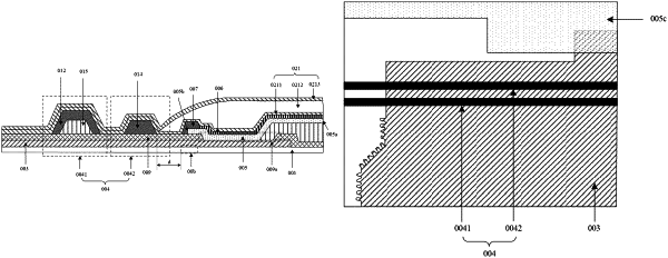
1. A display substrate, comprising:
a base substrate;
a plurality of pixel units located on the base substrate;
at least one first power line located on the base substrate;
a barrier structure surrounding the plurality of pixel units;
an adapting structure comprising a first side face and a second side face opposite to the first side face, the first side face being closer to the plurality of pixel units than the second side face;
a cathode layer located on a side of the adapting structure distal from the base substrate; and
a first organic pattern located on the side of the adapting structure distal from the base substrate,
wherein one end of the at least one first power line is located on a side of the barrier structure distal from the plurality of pixel units, and is configured for receiving power signals; and the other end of the at least one first power line is located between the barrier structure and the plurality of pixel units, and is connected to the cathode layer through the adapting structure, and
wherein the first organic pattern covers at least a portion of the second side face, an orthographic projection of the first organic pattern on the base substrate and an orthographic projection of the at least one first power line on the base substrate overlap at a first overlapping region, and the first overlapping region and an orthographic projection of the barrier structure on the base substrate do not overlap,
wherein a plurality of tooth-shaped protruding structures are provided on a side face of the at least one first power line at the end of the barrier structure distal from the plurality of pixel units,
wherein an orthographic projection of the protruding structures on the base substrate and the orthographic projection of the barrier structure on the base substrate do not overlap.
|
|
16. A display substrate, comprising:
a base substrate;
a plurality of pixel units located on the base substrate;
at least one power line located on the base substrate;
a barrier structure surrounding the plurality of pixel units, wherein an orthographic projection of the power line on the base substrate passes across an orthographic projection of the barrier structure on the base substrate;
an adapting structure comprising a first side face and a second side face opposite to the first side face, wherein the first side face is closer to the plurality of pixel units than the second side face;
a cathode layer located on a side of the adapting structure distal from the base substrate;
a first organic pattern located on the side of the adapting structure distal from the base substrate; and
a passivation layer covering the at least one power line,
wherein an opening is further provided in the passivation layer, the adapting structure is connected to the at least one power line through the opening at a side proximal to the base substrate, and the adapting structure is connected to the cathode layer at a side distal from the base substrate,
wherein a plurality of tooth-shaped protruding structures are provided on a side face of the at least one power line at the end of the barrier structure distal from the plurality of pixel units,
wherein an orthographic projection of the protruding structures on the base substrate and the orthographic projection of the barrier structure on the base substrate do not overlap.
|
|
18. A display substrate, comprising:
a base substrate;
a plurality of pixel units located on the base substrate;
at least one first power line located on the base substrate;
a barrier structure surrounding the plurality of pixel units;
an adapting structure comprising a first side face and a second side face opposite to the first side face, the first side face being closer to the plurality of pixel units than the second side face;
a cathode layer located on a side of the adapting structure distal from the base substrate; and
a first organic pattern located on the side of the adapting structure distal from the base substrate,
wherein one end of the at least one first power line is located on a side of the barrier structure distal from the plurality of pixel units, and is configured for receiving power signals; and the other end of the at least one first power line is located between the barrier structure and the plurality of pixel units, and is connected to the cathode layer through the adapting structure, and
wherein the first organic pattern covers at least a portion of the second side face, an orthographic projection of the first organic pattern on the base substrate and an orthographic projection of the at least one first power line on the base substrate overlap at a first overlapping region, and the first overlapping region and an orthographic projection of the barrier structure on the base substrate do not overlap,
wherein the at least one first power line comprises: a first metal layer; the display substrate further comprises: an auxiliary metal layer located on a side of the first metal layer distal from the base substrate; and
the auxiliary metal layer is in contact with the adapting structure at a side distal from the first metal layer, and an orthographic projection of the auxiliary metal layer on the base substrate and an orthographic projection of the barrier structure on the base substrate do not overlap.
|