| CPC H10K 59/1213 (2023.02) [H10K 59/131 (2023.02)] | 20 Claims |

|
1. An array substrate comprising:
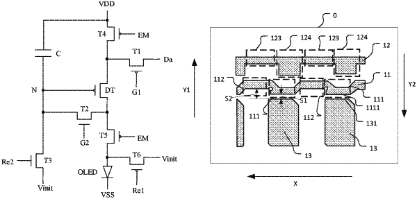
a pixel driving circuit and a data line, wherein the pixel driving circuit comprises a driving transistor, a first transistor connected between a first electrode of the driving transistor and the data line, a second transistor connected between a gate electrode and a second electrode of the driving transistor, the driving transistor and the first transistor are P-type transistors, and the second transistor is a N-type transistor; and
a base substrate and a first conductive layer arranged at a side of the base substrate, the base substrate comprising:
a first conductive portion for forming the gate electrode of the driving transistor;
a first gate line at a side of the first conductive portion, a part of the first gate line being configured to form a gate electrode of the first transistor; and
a second gate line at a side of the first gate line away from the first conductive portion, a part of the second gate line being configured to form a first gate electrode of the second transistor.
|