| CPC H10K 59/121 (2023.02) [H10K 50/844 (2023.02); H10K 59/131 (2023.02); H10K 59/65 (2023.02)] | 19 Claims |

|
1. A display panel, comprising:
a base substrate; and
pixel circuits arranged in an array on the base substrate, wherein each row of pixel circuits comprises a gate line extending in a row direction, each column of pixel circuits comprises a data line extending in a column direction, the gate line and the data line are disposed on different layers,
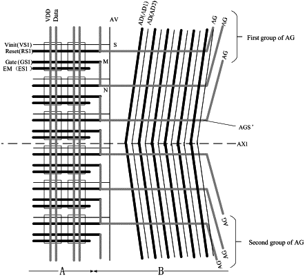
wherein the display panel comprises a light transmittance region and a display region around the light transmittance region, the pixel circuits are disposed in the display region, the gate line of each row of m rows of pixel circuits is divided into a first gate line portion and a second gate line portion by the light transmittance region, the first gate line portion is connected to the second gate line portion by an auxiliary gate line, at least part of the auxiliary gate line extends along an edge of the light transmittance region, wherein m is a natural number and m≥2,
wherein the data line of each column of n columns of pixel circuits is divided into a first data line portion and a second data line portion by the light transmittance region, the first data line portion is connected to the second data line portion by an auxiliary data line, wherein n is a natural number and n≥2,
wherein the auxiliary gate line comprises an auxiliary gate line sub-portion, the auxiliary gate line sub-portion and the auxiliary data line have an overlapped region,
wherein the m rows of pixel circuits comprise at least two rows of pixel circuits, an overlapped area of the auxiliary gate line sub-portion of the auxiliary gate line for connecting the first gate line portion and the second gate line portion in one row of the at least two rows of pixel circuits and the auxiliary data line is different from an overlapped area of the auxiliary gate line sub-portion of the auxiliary gate line for connecting the first gate line portion and the second gate line portion in the other one row of the at least two rows of pixel circuits and the auxiliary data line,
wherein each row of pixel circuits further comprises a reset signal line extending in the row direction, the reset signal line and the gate line are disposed in the same layer and parallel to each other, the reset signal line of each row of the m rows of pixel circuits is divided into a first reset signal line portion and a second reset signal line portion by the light transmittance region,
wherein in the m rows of pixel circuits, the first reset signal line portion of the ith row of pixel circuits is electrically connected to the first gate line portion of the i−1th row of pixel circuits, the second reset signal line portion of the ith row of pixel circuits is electrically connected to the second gate line portion of the i−1th row of pixel circuits, wherein i is a natural number, and 1<i≤m.
|