| CPC H10K 50/822 (2023.02) [H10K 71/00 (2023.02); H10K 71/621 (2023.02); H10K 2102/351 (2023.02)] | 17 Claims |

|
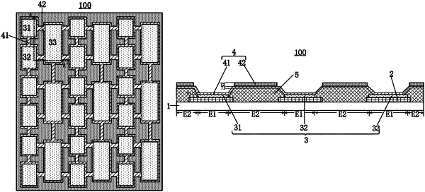
1. An array substrate comprising:
a base substrate;
a plurality of light emitting layers arranged on the base substrate along a row direction and a column direction; and
a first electrode on a side of the plurality of light emitting layers away from the base substrate,
wherein the array substrate comprises a light emitting area and a non-light emitting area, the first electrode comprises a stacked first sub-electrode layer and a second sub-electrode layer, the first sub-electrode layer is in the light emitting area and the non-light emitting area, and the second sub-electrode layer is only in the non-light emitting area, and a thickness of a portion of the first electrode in the light emitting area is less than a thickness of a portion of the first electrode in the non-light emitting area,
wherein an orthographic projection of the second sub-electrode layer on the base substrate does not overlap with an orthographic projection of each of the light emitting layers on the base substrate,
wherein a width of a first portion of the first sub-electrode layer in the light-emitting area is greater than a width of a second portion of the first sub-electrode layer in the non-light emitting area, and
wherein the second sub-electrode layer comprises a plurality of patterned layers, two adjacent light emitting layers of the plurality of light emitting layers are spaced by two patterned layers of the plurality of patterned layers which are disconnected from each other.
|