| CPC H10B 61/22 (2023.02) [G11C 11/161 (2013.01); H01L 23/5226 (2013.01); H01L 23/5283 (2013.01); H10N 50/01 (2023.02); H10N 50/10 (2023.02); H10N 50/80 (2023.02)] | 20 Claims |

|
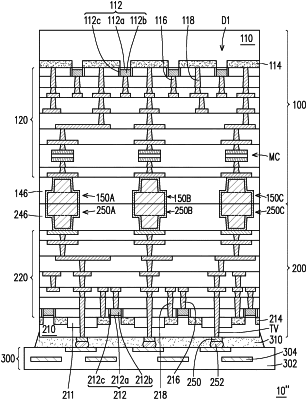
1. A semiconductor package, comprising:
a first semiconductor device, comprising:
a first semiconductor substrate;
a first bonding structure in a first dielectric layer; and
a memory cell between the first semiconductor substrate and the first bonding structure, wherein the memory cell is a MRAM cell; and
a second semiconductor device stacked over the first semiconductor device, comprising:
a second semiconductor substrate;
a second bonding structure in a second dielectric layer; and
a peripheral circuit between the second semiconductor substrate and the second bonding structure,
wherein the first bonding structure and the second bonding structure are bonded and disposed between the memory cell and the peripheral circuit, and the memory cell and the peripheral circuit are electrically connected through the first bonding structure and the second bonding structure.
|