| CPC H10B 51/20 (2023.02) [H01L 29/41741 (2013.01); H01L 29/41775 (2013.01); H10B 51/00 (2023.02); H10B 51/10 (2023.02); H10B 51/30 (2023.02)] | 20 Claims |

|
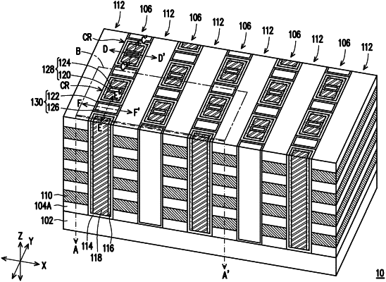
1. A memory device, comprising:
a first stacking structure comprising a plurality of first gate layers and a second stacking structure comprising a plurality of second gate layers, standing on a substrate and separated from each other through a trench;
a plurality of cell regions, disposed in the trenches and separated from each other, wherein the plurality of cell regions extend along a stacking direction of the plurality of first gate layers comprised in the first stacking structure;
gate dielectric layers, disposed in the plurality of cell regions and lining sidewalls of the plurality of cell regions, wherein the gate dielectric layers cover portions of the substrate overlapped with the plurality of cell regions;
channel layers, disposed in the plurality of cell regions and each lining a sidewall of a respective one of the gate dielectric layers;
conductive pillars, disposed in the plurality of cell regions and extending along the stacking direction, wherein every two conductive pillars are placed into a respective one cell region; and
a plurality of isolators, disposed in the plurality of cell regions and extending along the stacking direction, wherein the every two conductive pillars are separated from one another by a respective one of the plurality of isolators, and each of the plurality of isolators comprise:
a main layer, extending along the stacking direction; and
a liner, surrounding the main layer, wherein the liner separates the main layer from the every two conductive pillars and a respective one of the channel layers in each of the cell regions.
|