| CPC H10B 43/27 (2023.02) [H10B 41/27 (2023.02); H10B 41/35 (2023.02); H10B 41/41 (2023.02); H10B 43/35 (2023.02); H10B 43/40 (2023.02)] | 32 Claims |
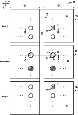
|
1. An integrated assembly, comprising:
a memory region and another region adjacent the memory region;
channel-material-pillars arranged within the memory region, and conductive posts arranged within said other region;
a source structure coupled to lower regions of the channel-material-pillars;
a panel extending across the memory region and said other region, and separating a first memory-block-region from a second memory-block-region;
doped-semiconductor-material directly adjacent to the panel within the memory region and the other region; the doped-semiconductor-material being at least part of the source structure within the memory region;
liners directly adjacent to the conductive posts and laterally surrounding the conductive posts; the liners being between the conductive posts and the doped-semiconductor-material; and
wherein the doped-semiconductor-material directly contacts the liners.
|