| CPC H10B 41/35 (2023.02) [H01L 29/40117 (2019.08); H01L 29/4234 (2013.01); H01L 29/66825 (2013.01); H01L 29/66833 (2013.01); H01L 29/7881 (2013.01); H01L 29/792 (2013.01); H10B 41/30 (2023.02); H10B 43/30 (2023.02); H10B 43/35 (2023.02)] | 20 Claims |

|
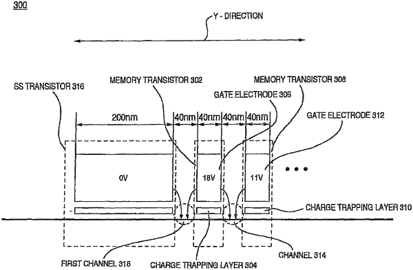
1. A device comprising:
a base layer;
a first memory transistor comprising:
a first gate electrode; and
a first charge trapping layer disposed between the base layer and the first gate electrode; and
a second memory transistor comprising:
a second gate electrode; and
a second charge trapping layer disposed between the base layer and the second gate electrode;
a source select transistor comprising:
a source select gate electrode;
wherein the source select transistor, the first memory transistor and the second memory transistor are disposed in a NAND string;
wherein the source select transistor is at one end of the NAND string, the first memory transistor is adjacent to the source select transistor and the second memory transistor is adjacent to the first memory transistor;
wherein the first memory transistor and the second memory transistor are separated by a first distance, which defines a first region;
wherein there is no diffusion region in the first region defined by the first distance;
wherein a conductive path is formed in the first region between the first and second memory transistors due to gate fringing field effects associated with the first and second memory transistors;
wherein the first memory transistor does not include a diffusion region for source and/or drain;
wherein the second memory transistor does not include a diffusion region for source and/or drain;
wherein the first memory transistor and source select transistor are separated by a second distance, which defines a second region;
wherein there is no diffusion region in the second region defined by the second distance;
wherein a conductive path is formed in the second region between the first memory transistor and the source select transistor due to gate fringing field effects associated with the first memory transistor and the source select transistor; and
wherein the source select transistor does not include a diffusion region for source and/or drain.
|