| CPC H10B 12/315 (2023.02) [H01L 23/5226 (2013.01); H01L 23/528 (2013.01); H01L 28/91 (2013.01); H10B 12/0335 (2023.02); H10B 12/05 (2023.02); H10B 12/318 (2023.02); H10B 12/482 (2023.02); H10B 12/485 (2023.02)] | 23 Claims |

|
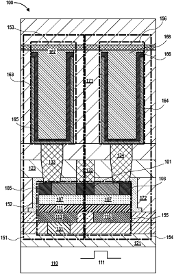
1. A memory device, comprising:
a first memory cell including a first storage cell and a first transistor to control access to the first storage cell;
a second memory cell including a second storage cell and a second transistor to control access to the second storage cell; and
a shared contact electrode that is shared between the first transistor and the second transistor, the shared contact electrode being coupled to a source area or a drain area of the first transistor, and coupled to a source area or a drain area of the second transistor, and further being coupled to a bit line of the memory device, wherein the shared contact is on a side of a first channel area and a second channel area opposite a first gate electrode and a second gate electrode of the first and second transistors, respectively, and wherein the first transistor further includes the first gate electrode coupled to a first word line, and the second transistor further includes the second gate electrode coupled to a second word line.
|