| CPC H05K 3/46 (2013.01) [H05K 1/0201 (2013.01); H05K 1/118 (2013.01); H05K 2201/10037 (2013.01)] | 19 Claims |

|
1. A method of fabricating a flexible interconnect circuit comprising a set of current controlling slits, the method comprising:
receiving a conductive layer design corresponding to a conductive layer of the flexible interconnect circuit, wherein the conductive layer design comprises design-contact-forming portions corresponding to contact-forming portions of the conductive layer;
determining a resistive heating map for the conductive layer based on an electric current map comprising target current values, wherein:
each of the target current values corresponds to one of the design-contact-forming portions and represents a maximum current to be flowed through a corresponding one of the contact-forming portions, and
the resistive heating map comprises heating rate values for different points in the conductive layer design; and
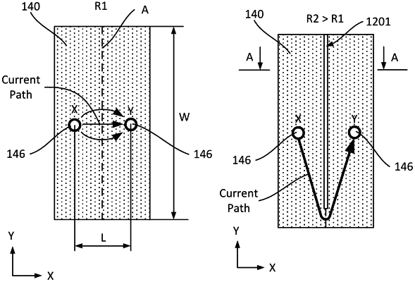
when any of the heating rate values in the resistive heating map falls outside of resistive-heating-map limits, adding or changing a design set of current controlling slits in the conductive layer design and determining the resistive heating map using the conductive layer design with the design set of current controlling slits until all of the heating rate values in the resistive heating map are within the resistive-heating-map limits; and
patterning the conductive layer in accordance with the conductive layer design comprising the design set of current controlling slits, wherein patterning the conductive layer comprises forming the set of current controlling slits corresponding to the design set of current controlling slits.
|