| CPC H05K 1/0298 (2013.01) [H05K 1/0218 (2013.01); H05K 1/0231 (2013.01); H05K 1/0242 (2013.01)] | 6 Claims |
|
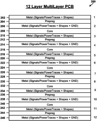
1. A multi-layer printed circuit board (PCB), comprising: a plurality of layers comprising:
a plurality of signal layers,
a plurality of ground plane layers,
a plurality of inner signal layers, and
a single core substrate layer,
wherein:
each individual layer in the plurality of layers is separated from its immediately adjacent layers by one or more prepreg substrate layers,
each of the one or more prepeg substrate layers is less rigid than the single core substrate layer,
the one or more prepeg substrate layers bond two or more of the prepreg separated individual layers together, and
the prepreg-separated individual layers include the plurality of signal layers, the plurality of ground plane layers, and the plurality of inner signal layers.
|