| CPC H05K 1/0237 (2013.01) [H05K 1/092 (2013.01); H05K 3/0035 (2013.01); H05K 3/022 (2013.01); H05K 3/423 (2013.01); H05K 3/4644 (2013.01); H05K 2201/0355 (2013.01); H05K 2201/09563 (2013.01)] | 10 Claims |
|
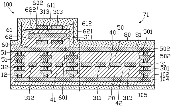
1. A circuit board for transmitting high-frequency signal, comprising:
a first circuit board comprising a first conductive wiring layer, a first base layer, and a second conductive wiring layer stacked in that order;
a second circuit board comprising a second base layer and a third conductive wiring layer stacked together, the third layer comprising at least one power line, at least one signal line, at least two first ground lines, at least one second ground lines, the signal line and the control line disposed at opposite sides of the power line, the first ground lines disposed at opposite sides of the signal line, the second ground line disposed at a side of the control line away from the power line, the second circuit board divided into a first region containing the signal line and a second region besides the first region, the second region the power line and the control line disposed in the second region;
at least one third circuit board each comprising a third base layer and a fourth conductive wiring layer stacked together;
a fourth circuit board comprising a fourth base layer and a fifth conductive wiring layer stacked together, the fifth conductive wiring layer comprising at least one power line or at least one control line;
a sixth circuit board comprising a sixth base layer and a seventh conductive wiring layer stacked together;
a fifth circuit board comprising a fifth base layer and a sixth conductive wiring layer stacked together, and the sixth conductive wiring layer comprising at least one power line or at least one control line;
wherein the first circuit board, the second circuit board, the third circuit boards are stacked in that order, the fourth circuit board, the sixth circuit board, and the fifth circuit board are disposed on the third circuit board and correspond to the first region, the sixth circuit board is disposed between the fourth circuit board and the fifth circuit board.
|