US 11,950,356 B2
Mating backplane for high speed, high density electrical connector
Mark W. Gailus, Concord, MA (US); Marc B. Cartier, Jr., Durham, NH (US); Vysakh Sivarajan, Nashua, NH (US); and David Levine, Amherst, NH (US)
Assigned to Amphenol Corporation, Wallingford, CT (US)
Filed by Amphenol Corporation, Wallingford, CT (US)
Filed on Dec. 13, 2022, as Appl. No. 18/079,956.
Application 18/079,956 is a continuation of application No. 17/082,105, filed on Oct. 28, 2020, granted, now 11,546,983.
Application 17/082,105 is a continuation of application No. 16/578,637, filed on Sep. 23, 2019, granted, now 10,849,218, issued on Nov. 24, 2020.
Application 16/578,637 is a continuation of application No. 16/032,284, filed on Jul. 11, 2018, granted, now 10,455,689, issued on Oct. 22, 2019.
Application 16/032,284 is a continuation of application No. 15/792,953, filed on Oct. 25, 2017, granted, now 10,034,366, issued on Jul. 24, 2018.
Application 15/792,953 is a continuation of application No. 14/947,166, filed on Nov. 20, 2015, granted, now 9,807,869, issued on Oct. 31, 2017.
Claims priority of provisional application 62/190,590, filed on Jul. 9, 2015.
Claims priority of provisional application 62/172,854, filed on Jun. 9, 2015.
Claims priority of provisional application 62/172,849, filed on Jun. 9, 2015.
Claims priority of provisional application 62/082,905, filed on Nov. 21, 2014.
Prior Publication US 2023/0113153 A1, Apr. 13, 2023
Int. Cl. H05K 1/02 (2006.01); H01R 43/20 (2006.01); H05K 1/11 (2006.01); H05K 3/00 (2006.01); H05K 3/40 (2006.01); H05K 3/42 (2006.01)
CPC H05K 1/0222 (2013.01) [H01R 43/205 (2013.01); H05K 1/0216 (2013.01); H05K 1/0219 (2013.01); H05K 1/025 (2013.01); H05K 1/0251 (2013.01); H05K 1/0253 (2013.01); H05K 1/0298 (2013.01); H05K 1/115 (2013.01); H05K 3/0047 (2013.01); H05K 3/4038 (2013.01); H05K 3/429 (2013.01); H05K 2201/07 (2013.01); H05K 2201/09063 (2013.01); H05K 2201/09318 (2013.01); H05K 2201/09545 (2013.01); H05K 2201/096 (2013.01); H05K 2201/097 (2013.01); H05K 2201/09718 (2013.01); H05K 2201/09845 (2013.01); H05K 2201/09854 (2013.01); H05K 2201/10189 (2013.01)] 18 Claims
OG exemplary drawing
 
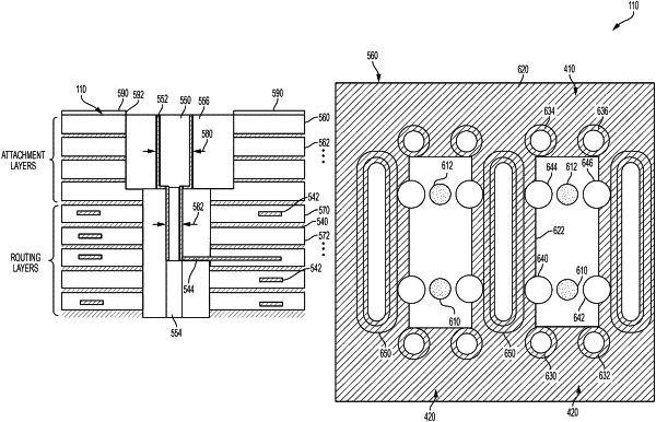
1. A printed circuit board comprising:
a plurality of layers including conductive layers separated by dielectric layers; and
via patterns formed in one or more of the plurality of layers, each of the via patterns comprising:
first and second signal vias connecting to respective signal traces on one or more of the plurality of layers;
ground vias extending through at least some layers of the plurality of layers; and
at least one shadow via extending through at least some layers of the plurality of layers, wherein the at least one shadow via is plated or filled with a conductive material and wherein the at least one shadow via is located on a first line that passes through one of the first and second signal vias, the first line being perpendicular to a second line that passes through the first and second signal vias.