| CPC H05K 1/0219 (2013.01) [H05K 1/0224 (2013.01); H05K 1/028 (2013.01)] | 16 Claims |

|
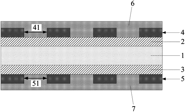
1. A flexible circuit board, comprising:
a substrate layer;
a first conductive layer, located on a first surface of the substrate layer and comprising:
a plurality of first traces; and
a first conductive portion;
wherein the first conductive portion is insulated from the first traces and is grounded;
a second conductive layer, located on a second surface, opposite to the first surface, of the substrate layer and comprising:
a plurality of second traces; and
a second conductive portion;
wherein the second conductive portion is insulated from the second traces and is grounded;
a first cover film, located on a side of the first conductive layer facing away from the substrate layer, a part of the first cover film overlapping the first conductive portion being provided with:
a plurality of first hollow portions;
a second cover film, located on a side of the second conductive layer facing away from the substrate layer, a part of the second cover film overlapping the second conductive portion being provided with:
a plurality of second hollow portions;
wherein an orthographic projection of each of the first hollow portions on the substrate layer has an overlapping area with an orthographic projection of at least one of the second hollow portions on the substrate layer;
a first electromagnetic shielding layer, located on a side of the first cover film facing away from the substrate layer, the first electromagnetic shielding layer being coupled to the first conductive portion through the first hollow portions; and
a second electromagnetic shielding layer, located on a side of the second cover film facing away from the substrate layer, the second electromagnetic shielding layer being coupled to the second conductive portion through the second hollow portions.
|