| CPC H04L 25/03057 (2013.01) [G06F 3/05 (2013.01); G06F 3/0604 (2013.01); G06F 3/0644 (2013.01); G06F 3/0673 (2013.01); G11C 19/00 (2013.01); H04L 25/03146 (2013.01); H04L 25/03878 (2013.01)] | 13 Claims |
|
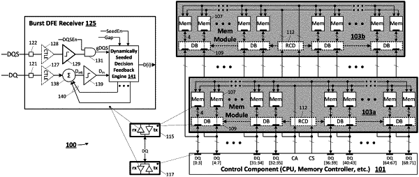
1. A method of operation within an integrated-circuit buffer component (buffer IC), the method comprising:
sampling a signaling link during each of a sequence of sampling intervals to generate a corresponding sequence of data bits, including resolving each of the data bits to a logic state according to voltage levels, during the sampling interval, of both the signaling link and an equalization signal;
generating the equalization signal for each of the sampling intervals based on either (i) the logic state of one or more previously generated data bits or (ii) one or more bit values having predetermined logic states, depending on whether the sampling interval is preceded by a time period in which no data is conveyed to the buffer IC via the signaling link; and
outputting the sequence of data bits from the buffer IC to a memory component.
|