US 11,949,390 B2
Load modulated balanced power amplifier integrated circuits including transformer-based hybrid splitter/combiner circuits
Tushar Sharma, Princeton, NJ (US); Chandrakanth Chappidi, Princeton, NJ (US); Zheng Liu, Monmouth Junction, NJ (US); and Kaushik Sengupta, Princeton Junction, NJ (US)
Assigned to The Trustees of Princeton University, Princeton, NJ (US)
Filed by The Trustees of Princeton University, Princeton, NJ (US)
Filed on Jan. 15, 2021, as Appl. No. 17/150,936.
Claims priority of provisional application 62/961,501, filed on Jan. 15, 2020.
Prior Publication US 2021/0218375 A1, Jul. 15, 2021
Int. Cl. H03F 1/02 (2006.01); H03F 3/24 (2006.01)
CPC H03F 3/245 (2013.01) [H03F 1/0288 (2013.01); H03F 2200/216 (2013.01); H03F 2200/534 (2013.01)] 12 Claims
OG exemplary drawing
 
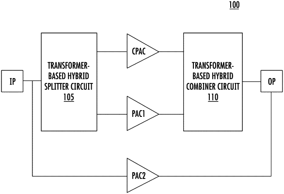
1. A load modulated balanced amplifier (LMBA) circuit, comprising:
an input pad of the LMBA circuit configured to receive an input signal on a semiconductor die;
a transformer-based hybrid splitter coupled to the input pad and configured to provide a first split input signal and a second split input signal from the input signal;
a control power amplifier circuit coupled the first split input signal; and
a power amplifier circuit coupled to the second split input signal.