| CPC H02M 1/4208 (2013.01) [H02M 1/126 (2013.01); H02M 1/44 (2013.01)] | 7 Claims |

|
1. A power factor correction circuit comprising:
a global voltage input; and
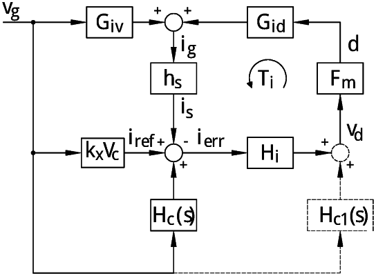
means for deriving a reference current from the global voltage, the means for deriving including first and second power stages defining two branches, a first branch drawing a current in phase with a load voltage and a second branch drawing a leading phase current which combine to derive the reference current from the global voltage;
whereby the means for deriving the reference current comprises a leading phase admittance cancellation (LPAC) transfer function and a filter, whereby the reference current is derived from a sum of an output of the LPAC transfer function and an output of the filter, such that the power factor correction circuit has a closed-loop admittance transfer function of:
 where the filter has the form:
 where:
ig is a global current;
vs is a global voltage;
Giv is a first power stage transfer function;
Gid is a second power stage transfer function;
Fm is a modulator gain;
kx is an input voltage gain;
Vc is an output of a voltage loop in the power factor correction circuit; and
Vo is a DC voltage.
|