| CPC H02J 50/80 (2016.02) [H02J 50/40 (2016.02); H02J 50/50 (2016.02)] | 11 Claims |

|
1. A contactless device, comprising:
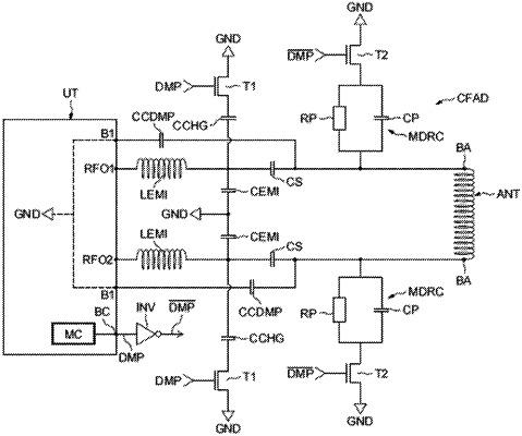
an impedance matching and filter circuit connected to an antenna;
a control circuit configured to modify the impedance matching and filter circuit to have a first configuration in support of the contactless device operating to carry out a contactless communication with a second device during a communications session and to modify the impedance matching and filter circuit to have a second configuration in support of the contactless device operating to carry out said contactless charging of a third device during a charging session;
wherein the contactless device comprises a processing unit possessing first and second output terminals coupled to corresponding first and second terminals of said antenna through said impedance matching and filter circuit;
wherein said impedance matching and filter circuit comprises:
a first inductor connected between the first output terminal and a first intermediate node;
a second inductor connected between the second output terminal and a second intermediate node;
a first capacitor connected between the first intermediate node and a ground node;
a second capacitor connected between the second intermediate node and the ground node;
a third capacitor connected between the first intermediate node and the first terminal of the antenna;
a fourth capacitor connected between the second intermediate node and the second terminal of the antenna;
a fifth capacitor connected between the first terminal of the antenna and the ground node;
a sixth capacitor connected between the second terminal of the antenna and the ground node;
a seventh capacitor and first switch connected in series between the first intermediate node and the ground node;
an eighth capacitor and second switch connected in series between the first second intermediate node and the ground node;
wherein said first and second switches are open when in the first configuration and closed when in the second configuration;
a first parallel resistor-capacitor circuit and third switch connected in series between the first antenna terminal and the ground node;
a second parallel resistor-capacitor circuit and fourth switch connected in series between the second antenna terminal and the ground node;
wherein said third and fourth switches are closed when in the first configuration and open when in the second configuration.
|