| CPC H02H 11/003 (2013.01) [H02J 7/0034 (2013.01)] | 7 Claims |
|
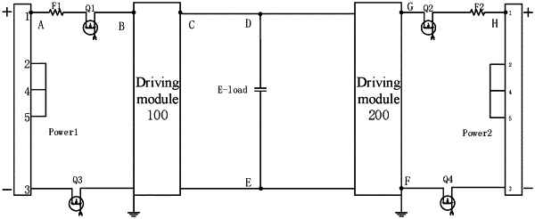
1. A direct-current power supply parallel input anti-reverse-connection circuit, comprising: a first power supply, a second power supply, a first switching tube, a second switching tube, a first driving module, and a second driving module; wherein
a first end of the first switching tube is configured to be connected with a positive end of the first power supply, and a second end of the first switching tube is connected with a positive input end of the first driving module;
a negative input end of the first driving module is configured to be connected with a negative end of the first power supply, wherein the negative input end of the first driving module is a grounding end;
the first driving module converts a power supply and provides the converted power supply to a load;
a first end of the second switching tube is configured to be connected with a positive end of the second power supply, and a second end of the second switching tube is connected with a positive input end of the second driving module;
a negative input end of the second driving module is configured to be connected with a negative end of the second power supply, wherein the negative input end of the second driving module is a grounding end;
the second driving module converts a power supply and then provides the converted power supply to the load;
wherein, when the second power supply is reversely connected, the first switching tube is turned on, and the second switching tube is turned off, so as to prevent a current from flowing to the negative end of the second power supply from the positive end of the first power supply; and when the first power supply is reversely connected, the first switching tube is turned off, and the second switching tube is turned on so as to prevent a current from flowing to the negative end of the first power supply from the positive end of the second power supply;
wherein, the first switching tube is a first N-channel Metal Oxide Semiconductor (NMOS) tube; and
a source electrode of the first NMOS tube is configured to be connected with the positive end of the first power supply, a drain electrode of the first NMOS tube is connected with the positive input end of the first driving module, and a gate electrode of the first NMOS tube is connected with a first driving circuit, wherein the first driving circuit provides a high level for the gate electrode of the first NMOS tube.
|