| CPC H01L 33/62 (2013.01) [H01L 33/0095 (2013.01); H01L 33/58 (2013.01); H01L 2933/0058 (2013.01); H01L 2933/0066 (2013.01)] | 10 Claims |

|
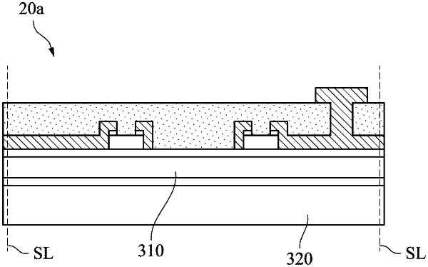
1. A light emitting diode packaging structure, comprising:
a flexible substrate;
a first adhesive layer disposed on the flexible substrate;
a plurality of micro light emitting elements disposed on the first adhesive layer, wherein the plurality of micro light emitting elements has a first surface facing to the first adhesive layer and a second surface opposite to the first surface, and the plurality of micro light emitting elements includes a red micro light emitting element, a blue micro light emitting element, and a green micro light emitting element;
a conductive pad disposed on the second surface of the micro light emitting element;
a redistribution layer covering the micro light emitting elements and the conductive pad, wherein the redistribution layer comprises an insulating layer and a circuit layer embedded in the insulating layer, and the circuit layer is electrically connected to the conductive pad; and
an electrode pad disposed on the redistribution layer and electrically connecting to the circuit layer, wherein a thickness of the flexible substrate is less than 100 um.
|