| CPC H01L 33/62 (2013.01) [H01L 25/0753 (2013.01); H01L 25/167 (2013.01); H01L 33/22 (2013.01); H01L 33/46 (2013.01); H01L 33/54 (2013.01); H01L 33/58 (2013.01)] | 19 Claims |

|
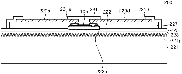
1. A unit pixel, comprising:
a transparent substrate;
a plurality of light emitting devices arranged on the transparent substrate;
a plurality of connection layers electrically connected to the plurality of light emitting devices such that each light emitting device is electrically connected to each corresponding connection layer and a common connection layer of the plurality of connection layers; and
a plurality of bonding pads disposed over the plurality of connection layers, and electrically connected to the plurality of connection layers;
a light blocking layer disposed on the transparent substrate;
an adhesive layer disposed on the transparent substrate and configured to cover a region of the light blocking layer; and
a surface layer disposed between the transparent substrate and the light blocking layer,
wherein:
the light blocking layer has windows through which light generated from the plurality of light emitting devices passes, and
the plurality of light emitting devices are disposed to correspond to the windows.
|