| CPC H01L 33/44 (2013.01) [G09F 9/30 (2013.01); H01L 27/15 (2013.01); H01L 27/156 (2013.01); H01L 33/36 (2013.01); H01L 33/38 (2013.01); H05B 33/10 (2013.01); H05B 33/12 (2013.01)] | 20 Claims |

|
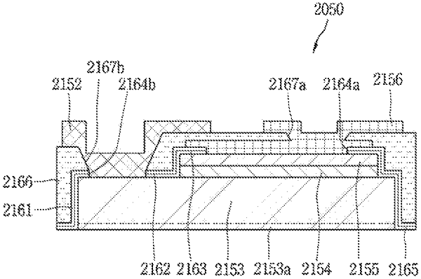
1. A display device comprising:
a plurality of semiconductor light emitting elements mounted on a substrate,
wherein at least one of the semiconductor light emitting elements comprises:
a first electrode and a second electrode spaced apart from each other;
a first conductivity type semiconductor layer disposed with the first electrode;
a second conductivity type semiconductor layer configured to overlap with the first conductivity type semiconductor layer, and disposed with the second electrode;
a first passivation layer covering outer surfaces of the first conductivity type semiconductor layer and the second conductivity type semiconductor layer; and
a second passivation layer coveting the first passivation layer,
wherein the first conductivity type semiconductor layer is disposed higher than the second conductivity type semiconductor layer, and
wherein at least one portion of the second electrode is overlapped with at least one portion of the first electrode along a thickness direction of the at least one semiconductor light emitting element.
|