US 11,949,045 B2
Light emitting element structure and method of fabricating a light emitting element
Hyun Min Cho, Seoul (KR); Jung Hong Min, Pyeongtaek-si (KR); Dae Hyun Kim, Hwaseong-si (KR); Dong Uk Kim, Hwaseong-si (KR); and Jae Hoon Jung, Seoul (KR)
Assigned to Samsung Display Co., Ltd., Yongin-si (KR)
Appl. No. 17/290,682
Filed by Samsung Display Co., Ltd., Yongin-si (KR)
PCT Filed May 27, 2019, PCT No. PCT/KR2019/006323
§ 371(c)(1), (2) Date Apr. 30, 2021,
PCT Pub. No. WO2020/091171, PCT Pub. Date May 7, 2020.
Claims priority of application No. 10-2018-0131072 (KR), filed on Oct. 30, 2018.
Prior Publication US 2022/0013693 A1, Jan. 13, 2022
Int. Cl. H01L 33/44 (2010.01); H01L 27/15 (2006.01); H01L 33/00 (2010.01); H01L 33/24 (2010.01)
CPC H01L 33/44 (2013.01) [H01L 27/156 (2013.01); H01L 33/0093 (2020.05); H01L 33/24 (2013.01); H01L 2933/0025 (2013.01)] 19 Claims
OG exemplary drawing
 
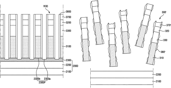
1. A method of fabricating a light-emitting element, the method comprising:
preparing a lower substrate, which includes a substrate and a separation layer on the substrate;
preparing at least one semiconductor rod on the separation layer;
forming a rod structure, which includes a rod protecting layer on the separation layer to surround the at least one semiconductor rod;
forming an auxiliary layer on at least part of the rod protecting layer;
separating the rod structure from the lower substrate by removing the separation layer; and
separating the at least one semiconductor rod from the rod structure.