| CPC H01L 33/305 (2013.01) [H01L 33/0008 (2013.01); H01L 33/22 (2013.01); H01L 33/325 (2013.01)] | 13 Claims |

|
1. A micro light-emitting diode, comprising:
a first-type semiconductor layer having a first doping type;
a light-emitting layer over the first-type semiconductor layer;
a first-type electrode over the first-type semiconductor layer;
a second-type semiconductor layer having a second doping type over the light-emitting layer, wherein the second doping type is different from the first doping type;
a second-type electrode over the second-type semiconductor layer;
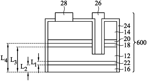
a barrier layer under the first-type semiconductor layer and away from the first-type electrode and the second-type electrode, wherein the barrier layer comprises a doped region having the second doping type; and
a third-type semiconductor layer having the first doping type under the barrier layer, wherein the barrier layer and the third-type semiconductor layer are both non-ohmic contact layers, wherein the first-type electrode penetrates the second-type semiconductor layer, the light-emitting layer and extends into the first-type semiconductor layer and is electrically connected to the first-type semiconductor layer, and wherein a thickness of the third-type semiconductor layer is a first thickness, and a total thickness of the first-type semiconductor layer, barrier layer, and third-type semiconductor layer is a second thickness, wherein a ratio of the first thickness to the second thickness is greater than 0.9.
|