| CPC H01L 31/1105 (2013.01) [H01L 31/03046 (2013.01); H01L 31/1844 (2013.01)] | 18 Claims |
|
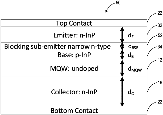
10. A method of forming an optical modulator comprising steps of:
forming an emitter layer with N-type doping having a first bandgap energy;
forming a base layer with P-type doping having a second bandgap energy;
forming a sub-emitter layer disposed between the emitter layer and the base layer, wherein the sub-emitter layer has a third bandgap energy that is less than both the first bandgap energy and the second bandgap energy;
forming a collector layer having n-type doping; and
forming an undoped layer disposed between the collector layer and the base layer, wherein the undoped layer is configured to have light propagate through the undoped region for modulation thereof.
|