| CPC H01L 31/107 (2013.01) [H01L 31/186 (2013.01)] | 19 Claims |
|
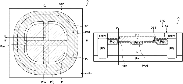
1. An integrated circuit, comprising:
a semiconductor well doped with a first type of dopant; and
a single photon avalanche diode (SPAD) in the semiconductor well, said SPAD including a PN junction between a first region doped with the first type of dopant and a second region doped with a second type of dopant opposite to the first type of dopant;
wherein the first region comprises:
a first sub-region positioned in contact with a bottom of the second region and centered with respect to the second region;
a second sub-region forming an annular volume laterally surrounding the first sub-region and separated from the first sub-region at a gap by a portion of said semiconductor well; and
a third sub-region that diametrically connects opposite portions of the annular volume for the second sub-region and is in contact with a bottom of the first sub-region.
|