US 11,949,034 B2
Photodetector with dual doped semiconductor material
John J. Ellis-Monaghan, Grand Isle, VT (US); Rajendran Krishnasamy, Essex Junction, VT (US); Siva P. Adusumilli, South Burlington, VT (US); and Ramsey Hazbun, Colchester, VT (US)
Assigned to GLOBALFOUNDRIES U.S. Inc., Malta, NY (US)
Filed by GLOBALFOUNDRIES U.S. Inc., Malta, NY (US)
Filed on Jun. 24, 2022, as Appl. No. 17/849,285.
Prior Publication US 2023/0420596 A1, Dec. 28, 2023
Int. Cl. H01L 31/105 (2006.01); H01L 31/0288 (2006.01); H01L 31/18 (2006.01); H01L 31/0216 (2014.01)
CPC H01L 31/105 (2013.01) [H01L 31/0288 (2013.01); H01L 31/1804 (2013.01); H01L 31/0216 (2013.01)] 20 Claims
OG exemplary drawing
 
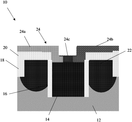
1. A structure comprising:
a photodetector; and
a semiconductor material on the photodetector, the semiconductor material comprising a first dopant type contacting a top surface of the photodetector, a second dopant type contacting the top surface of the photodetector and intrinsic semiconductor material contacting the top surface of the photodetector and separating the first dopant type from the second dopant type.