| CPC H01L 31/028 (2013.01) [H01L 31/0203 (2013.01); H01L 31/103 (2013.01); H01L 31/105 (2013.01); H01L 31/1808 (2013.01); H01L 31/1868 (2013.01)] | 20 Claims |

|
1. A method, comprising:
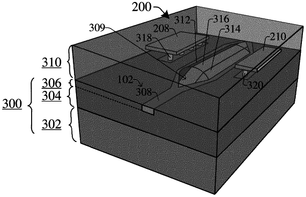
forming a trench in a substrate;
placing the substrate, including the trench, within a chamber, and epitaxially growing within the chamber a germanium layer having a curved upper surface in the trench, and in situ within the chamber, epitaxially growing a silicon cap layer over the germanium layer; and
forming a silicon germanium layer to overlie the germanium layer and before the silicon cap layer is formed, wherein the silicon germanium layer is formed in situ in the chamber in which the germanium layer was grown.
|