| CPC H01L 29/788 (2013.01) [H01L 21/28518 (2013.01); H01L 23/535 (2013.01); H01L 29/66825 (2013.01); H01L 29/66833 (2013.01); H01L 29/7889 (2013.01); H01L 29/792 (2013.01); H01L 29/7926 (2013.01); H10B 41/27 (2023.02); H10B 41/35 (2023.02); H10B 43/27 (2023.02); H10B 43/35 (2023.02)] | 12 Claims |

|
1. An electronic system comprising:
supervisory circuitry to generate memory control commands; and
at least one memory, coupled to the supervisory circuitry, to respond to the memory control commands, the at least one memory comprising:
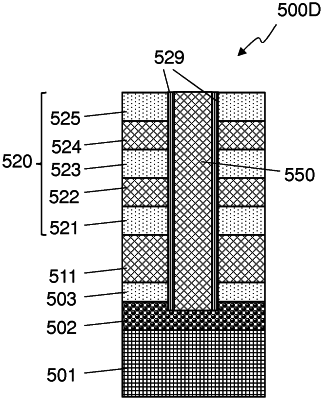
at least one source line over an upper surface of a substrate, the at least one source line having a vertical thickness and consisting of a heavily doped metallic silicide throughout the vertical thickness; and
two or more vertical NAND flash strings with select gates disposed over the source line, each of the two or more vertical NAND flash strings comprising insulating layers, conductive layers, and a pillar of semiconductor material extending through the insulating layers and conductive layers, and partially through one source line of the at least one source line, the pillar being in ohmic contact with the one source line.
|