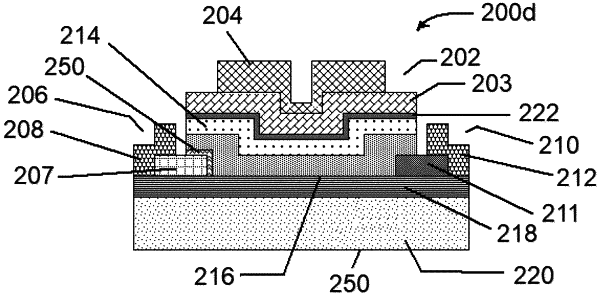
| CPC H01L 29/78618 (2013.01) [H01L 29/66969 (2013.01); H01L 29/78603 (2013.01); H01L 29/78642 (2013.01); H01L 29/7869 (2013.01)] | 30 Claims |

|
1. A vertical thin film transistor comprising:
a substantially planar substrate;
an insulating layer formed on the substrate;
a source formed on the insulating layer
a second insulating layer formed on the source, the second insulating layer forming a vertical well having an inner surface;
a source-channel interfacial member formed on the inner surface of the vertical well and the source;
an n-type semiconductor material formed on the source-channel interfacial member, such that the source is electrically connected to the n-type semiconductor material by the source-channel interfacial member;
a gate dielectric layer formed over the n-type semiconductor material;
a gate formed over the dielectric layer; and
a drain formed on the insulating layer and in electrical contact with the n-type semiconductor material, wherein when the transistor is in an on state current can flow from the source to the drain through the source-channel interfacial member and through a channel formed in the n-type semiconductor material.
|