| CPC H01L 29/78618 (2013.01) [H01L 21/0259 (2013.01); H01L 21/26513 (2013.01); H01L 21/2652 (2013.01); H01L 21/266 (2013.01); H01L 21/823807 (2013.01); H01L 21/823814 (2013.01); H01L 21/823864 (2013.01); H01L 27/092 (2013.01); H01L 29/0665 (2013.01); H01L 29/0673 (2013.01); H01L 29/161 (2013.01); H01L 29/24 (2013.01); H01L 29/42392 (2013.01); H01L 29/66545 (2013.01); H01L 29/66553 (2013.01); H01L 29/66636 (2013.01); H01L 29/66742 (2013.01); H01L 29/78696 (2013.01); H10B 10/125 (2023.02)] | 20 Claims |

|
1. A method of fabricating a semiconductor device, comprising:
providing a fin extending from a substrate;
forming a gate structure over the fin;
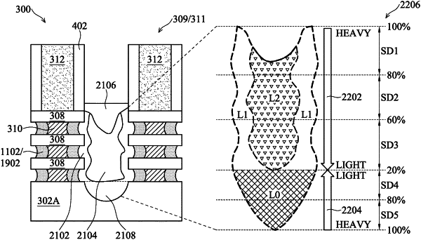
forming a source/drain feature within a source/drain region adjacent to the gate structure, wherein the source/drain feature includes a first epitaxial layer and a second epitaxial layer over the first epitaxial layer; and
doping the source/drain feature to provide a graded doping profile within the source/drain feature, wherein the graded doping profile is defined along a direction perpendicular to a top surface of the substrate;
wherein each of the first and second epitaxial layers include the graded doping profile, wherein the first epitaxial layer includes a graded carbon-doped layer, and wherein a first doping concentration of a bottom portion of the first epitaxial layer is greater than a second doping concentration of a top portion of the first epitaxial layer.
|