| CPC H01L 29/7851 (2013.01) [H01L 21/76229 (2013.01); H01L 21/823412 (2013.01); H01L 21/823431 (2013.01); H01L 21/823481 (2013.01); H01L 27/0629 (2013.01); H01L 27/0886 (2013.01); H01L 28/40 (2013.01); H01L 29/66795 (2013.01); H01L 29/7853 (2013.01)] | 20 Claims |

|
1. A method for forming a fin field effect transistor (FinFET) device structure, comprising:
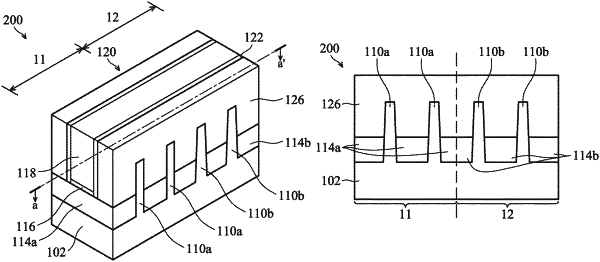
forming a first fin structure and a second fin structure in a first region of a substrate and a third fin structure and a fourth fin structure in a second region of the substrate, wherein the first fin structure and the second fin structure have a first sidewall surface and a second sidewall surface respectively, and the first sidewall surface and the second sidewall surface extend along a first direction, wherein the third fin structure and the fourth fin structure have a third sidewall surface and a fourth sidewall surface respectively, and the third sidewall surface and the fourth sidewall surface extend along a second direction different from the first direction;
forming an isolation layer covering top surfaces of the first fin structure, the second fin structure, the third fin structure and the fourth fin structure, wherein a first width of the isolation layer between top surfaces of the first fin structure and the second fin structure is different from a second width of the isolation layer between top surfaces of the third fin structure and the fourth fin structure;
etching a portion of the isolation layer to form an isolation structure to expose top portions of the first fin structure, the second fin structure, the third fin structure and the fourth fin structure;
wherein a first distance between top portions of the third sidewall surface of the third fin structure and the fourth sidewall surface of the fourth fin structure is greater than a second distance between top portions of the first sidewall surface of the first fin structure and the second sidewall surface of the second fin structure.
|