| CPC H01L 29/778 (2013.01) [H01L 29/1608 (2013.01); H01L 29/2003 (2013.01); H01L 29/66462 (2013.01)] | 20 Claims |

|
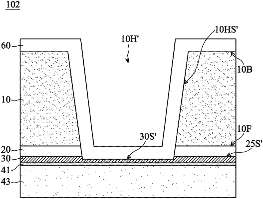
1. A semiconductor structure, comprising:
a substrate having a front side and a back side opposite the front side;
a first contact metal layer disposed on the front side of the substrate;
a second contact metal layer disposed on the first contact metal layer;
a third contact metal layer disposed on the second contact metal layer;
a III-V compound semiconductor layer disposed between the substrate and the first contact metal layer; and
a via hole penetrating through the substrate and the III-V compound semiconductor layer from the back side of the substrate, wherein a bottom of the via hole is defined by the first contact metal layer, and the first contact metal layer comprises molybdenum, tungsten, iridium, palladium, platinum, cobalt, ruthenium, osmium, rhodium, rhenium, or a combination thereof,
wherein the first contact metal layer, the second contact metal layer and the third contact metal layer overlap in a stacking direction.
|