| CPC H01L 29/7397 (2013.01) [H01L 21/31155 (2013.01); H01L 21/32 (2013.01); H01L 21/76816 (2013.01); H01L 29/66348 (2013.01); H01L 29/66674 (2013.01); H01L 29/7801 (2013.01)] | 20 Claims |
|
1. A power semiconductor device comprising a semiconductor body, the semiconductor body being coupled to a first load terminal and a second load terminal and configured to conduct a load current between the first and second load terminals, wherein the power semiconductor device further comprises:
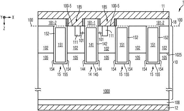
a first trench and a second trench that extend from a surface of the semiconductor body along a vertical direction, the first and second trenches laterally confining a mesa region along a first lateral direction;
a semiconductor source region of a first conductivity type and a semiconductor body region of a second conductivity type both being arranged in the mesa region adjacent to a trench sidewall of the first trench and electrically connected to the first load terminal, wherein the semiconductor source region is based on a first implantation material, and wherein the first trench is configured to induce an inversion channel in the semiconductor body region to control a load current in the mesa region; and
a first insulation layer arranged above the semiconductor body surface and having a plurality of insulation blocks, two of which laterally confine a contact hole of the first insulation layer,
wherein the first load terminal extends into the contact hole to contact both the semiconductor source region and the semiconductor body region at a surface of the mesa region,
wherein a first of the two insulation blocks laterally overlaps with the first trench and a second of the two insulation blocks laterally overlaps with the second trench,
wherein the first insulation block has a first lateral concentration profile of the first implantation material along the first lateral direction that is different from a second lateral concentration profile of the first implantation material along the first lateral direction present in the second insulation block.
|