| CPC H01L 29/7393 (2013.01) [H01L 29/0649 (2013.01); H01L 29/66325 (2013.01)] | 14 Claims |
|
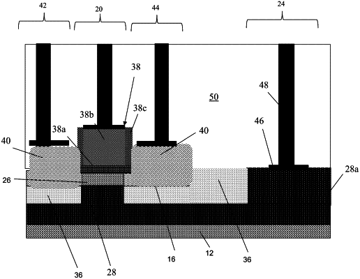
1. A structure comprising:
a base region comprising an undoped intrinsic base region and a doped extrinsic base region below the undoped intrinsic base region;
a raised emitter region on a first side of and above the doped extrinsic base region;
a raised collector region on a second side of and above the doped extrinsic base region;
a gate structure comprising a gate dielectric material and a gate control in a same channel region as the doped extrinsic base region, and sidewall spacers extending along sidewalls of the gate control; and
insulator material in a cavity of a semiconductor material part of which comprises the doped extrinsic base region and the undoped intrinsic base region, the insulator material surrounding the doped extrinsic base region and underneath both the raised emitter region and the raised collector region,
wherein the raised emitter region and the raised collector region extend above the gate dielectric material, and along the sidewall spacers of the gate structure, the sidewall spacers isolate the raised emitter region and the raised collector region from the gate control.
|