| CPC H01L 29/66818 (2013.01) [H01L 29/0847 (2013.01); H01L 29/66545 (2013.01); H01L 29/785 (2013.01); H01L 21/02233 (2013.01); H01L 21/02255 (2013.01); H01L 21/30604 (2013.01); H01L 21/3065 (2013.01); H01L 21/31111 (2013.01)] | 20 Claims |

|
1. A method comprising:
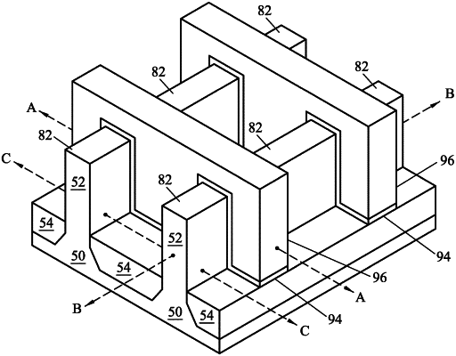
forming a dummy gate on a channel region of a semiconductor fin, the semiconductor fin protruding above an isolation region;
growing a source/drain region in the semiconductor fin adjacent the dummy gate;
depositing an etch stop layer on the source/drain region;
forming an inter-layer dielectric on the etch stop layer;
removing the dummy gate to expose the channel region of the semiconductor fin;
after removing the dummy gate, trimming the channel region by performing a plurality of oxidation and etch cycles, each of the oxidation and etch cycles removing a same amount of the channel region;
after trimming the channel region, forming a metal gate on the channel region, the metal gate extending along a sidewall of the channel region and along a top surface of the isolation region; and
forming a source/drain contact through the inter-layer dielectric and the etch stop layer, the source/drain contact coupled to the source/drain region, wherein the inter-layer dielectric and the etch stop layer are each between the source/drain contact and the metal gate.
|