| CPC H01L 29/41733 (2013.01) [H01L 21/02532 (2013.01); H01L 21/02576 (2013.01); H01L 21/02579 (2013.01); H01L 21/02603 (2013.01); H01L 21/30604 (2013.01); H01L 21/31111 (2013.01); H01L 21/76897 (2013.01); H01L 23/5286 (2013.01); H01L 29/0673 (2013.01); H01L 29/42392 (2013.01); H01L 29/45 (2013.01); H01L 29/66545 (2013.01); H01L 29/66553 (2013.01); H01L 29/66636 (2013.01); H01L 29/66742 (2013.01); H01L 29/78618 (2013.01); H01L 29/78696 (2013.01)] | 20 Claims |

|
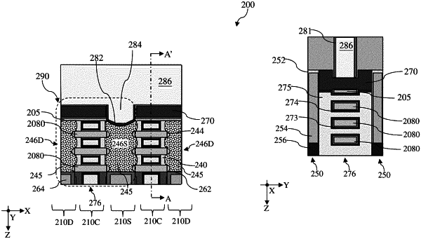
1. A semiconductor device, comprising:
a source feature and a drain feature;
a plurality of semiconductor nanostructures extending between the source feature and the drain feature along a horizontal direction and stacked one over another along a vertical direction;
a gate structure wrapping around each of the plurality of semiconductor nanostructures;
a bottom dielectric layer disposed directly over the gate structure and the drain feature;
a backside power rail disposed on the bottom dielectric layer and spanning directly over the source feature, the gate structure and the drain feature;
a backside source contact disposed directly between the source feature and the backside power rail along the vertical direction; and
a semiconductor bottom capping layer sandwiched between the bottom dielectric layer and the drain feature along the vertical direction,
wherein top surfaces of the drain feature and the gate structure are coplanar,
wherein the backside source contact extends completely through the bottom dielectric layer and partially into the source feature along the vertical direction such that a bottom surface of the backside source contact is lower than a bottom surface of the bottom dielectric layer,
wherein the backside power rail and the backside source contact are a continuous structure.
|