| CPC H01L 29/401 (2013.01) [H01L 21/02378 (2013.01); H01L 21/02527 (2013.01); H01L 21/0262 (2013.01); H01L 21/043 (2013.01); H01L 21/0485 (2013.01); H01L 29/165 (2013.01); H01L 29/45 (2013.01); H01L 29/1606 (2013.01); H01L 29/1608 (2013.01)] | 10 Claims |
|
1. A silicon carbide (SiC) ohmic contact preparation method, comprising:
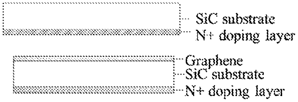
selecting a SiC substrate;
preparing a graphene/SiC structure by forming a graphene on a silicon-face (Si-face) of the SiC substrate;
depositing a gold (Au) film on the graphene of the graphene/SiC structure;
forming a first transfer electrode pattern on the Au film by a first photolithography;
etching the Au film uncovered by the first transfer electrode pattern through a wet etching;
etching the graphene uncovered by the Au film through a plasma etching after the wet etching;
forming a second transfer electrode pattern on the SiC substrate by a second photolithography; and
depositing an Au material on the Au film exposed by the second transfer electrode pattern and forming an Au electrode and then annealing, so as to obtain a SiC ohmic contact.
|