| CPC H01L 29/401 (2013.01) [H01L 21/28035 (2013.01); H01L 21/28088 (2013.01); H01L 21/823437 (2013.01); H01L 21/823462 (2013.01); H01L 21/823475 (2013.01); H01L 27/088 (2013.01); H01L 29/0665 (2013.01); H01L 29/42392 (2013.01); H01L 29/66545 (2013.01); H01L 29/66742 (2013.01); H01L 29/78645 (2013.01)] | 19 Claims |

|
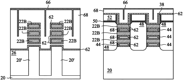
1. A method comprising:
forming a dummy gate stack over a semiconductor region;
forming epitaxial source/drain regions on opposite sides of the dummy gate stack;
removing the dummy gate stack to form a trench;
depositing a gate dielectric layer extending into the trench;
depositing a work-function layer over the gate dielectric layer, wherein the work-function layer comprises a seam therein;
depositing a silicon-containing layer to fill the seam, wherein at a time the depositing the silicon-containing layer is started, some portions of the seam are sealed by the work-function layer, and in a top view of the work-function layer, the seam is separated as discrete portions; and
performing a planarization process to remove excess portions of the silicon-containing layer, the work-function layer, and the gate dielectric layer, with remaining portions of the silicon-containing layer, the work-function layer, and the gate dielectric layer forming a gate stack.
|