| CPC H01L 29/0847 (2013.01) [H01L 21/823821 (2013.01); H01L 27/0924 (2013.01); H01L 29/42356 (2013.01); H01L 29/42368 (2013.01); H01L 29/66545 (2013.01); H01L 29/66636 (2013.01); H01L 29/66795 (2013.01); H01L 29/78 (2013.01); H01L 29/7833 (2013.01); H01L 29/7848 (2013.01); H01L 29/785 (2013.01); H01L 29/665 (2013.01)] | 9 Claims |

|
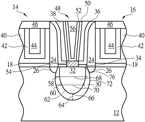
1. A method for fabricating semiconductor device, comprising:
forming a gate structure on a substrate;
forming a spacer around the gate structure;
forming a contact etch stop layer (CESL) directly contacting the spacer;
forming a buffer layer adjacent to the gate structure, wherein the buffer layer comprises a crescent moon shape and the buffer layer comprises an inner curve, an outer curve, and a planar surface connecting the inner curve and an outer curve along a top surface of the substrate, wherein the planar surface directly contacts the outer curve on an outer sidewall of the spacer;
forming an epitaxial layer on the buffer layer; and
forming a cap layer directly contacting a top surface of the epitaxial layer and between and directly contacting the CESL and the buffer layer, wherein the cap layer and the spacer are made of different materials.
|