| CPC H01L 29/0673 (2013.01) [H01L 21/02532 (2013.01); H01L 21/0262 (2013.01); H01L 21/3065 (2013.01); H01L 21/3086 (2013.01); H01L 21/31111 (2013.01); H01L 21/76224 (2013.01); H01L 21/823431 (2013.01); H01L 21/823437 (2013.01); H01L 21/823481 (2013.01); H01L 29/0847 (2013.01); H01L 29/0886 (2013.01); H01L 29/1033 (2013.01); H01L 29/401 (2013.01); H01L 29/42392 (2013.01); H01L 29/495 (2013.01); H01L 29/66545 (2013.01)] | 20 Claims |

|
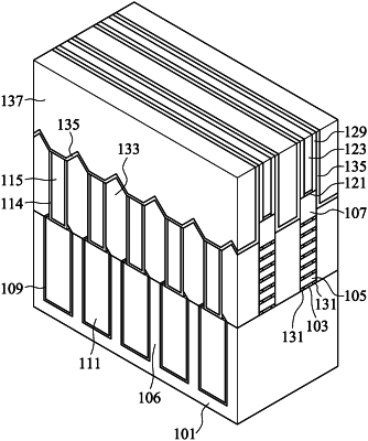
1. A method of forming a semiconductor device, the method comprising:
forming semiconductor strips protruding above a substrate;
forming isolation regions between adjacent ones of the semiconductor strips;
forming hybrid fins on the isolation regions;
forming a dummy gate structure over the semiconductor strips and the hybrid fins, wherein first portions of the hybrid fins are directly under the dummy gate structure, and second portions of the hybrid fins are beyond boundaries of the dummy gate structure;
forming source/drain regions over the semiconductor strips on opposing sides of the dummy gate structure;
removing the dummy gate structure;
forming nanowires over the semiconductor strips between the source/drain regions, wherein the nanowires are over and aligned with respective semiconductor strips; and
after forming the nanowires, reducing widths of the first portions of the hybrid fins while keeping widths of the second portions of the hybrid fins unchanged.
|