| CPC H01L 29/0649 (2013.01) [H01L 29/66795 (2013.01); H01L 29/785 (2013.01); H01L 29/78651 (2013.01)] | 20 Claims |

|
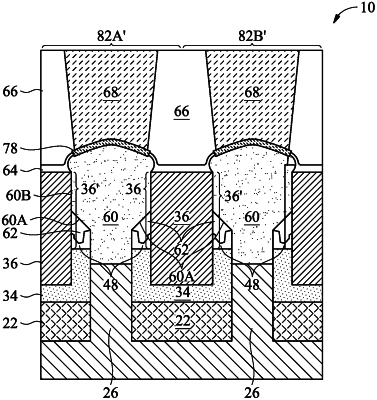
1. An integrated circuit device comprising:
a semiconductor substrate;
isolation regions over a bulk portion of the semiconductor substrate;
a semiconductor strip between opposite portions of the isolation regions;
a first dielectric fin and a second dielectric fin on opposite sides of the semiconductor strip, wherein the first dielectric fin and the second dielectric fin overlap, and are physically joined to, a first isolation region and a second isolation, respectively, of the isolation regions;
a semiconductor region over and contacting the semiconductor strip, wherein the semiconductor region extends laterally beyond edges of the semiconductor strip to contact the first dielectric fin and the second dielectric fin; and
an air gap between the semiconductor region and the first dielectric fin.
|