| CPC H01L 27/14643 (2013.01) [H01L 27/14603 (2013.01); H01L 27/14614 (2013.01); H01L 27/14616 (2013.01); H01L 27/14621 (2013.01); H01L 27/1463 (2013.01)] | 12 Claims |

|
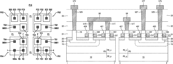
1. An image sensor comprising:
a semiconductor substrate;
a plurality of pillars, wherein each pillar of the plurality of pillars protrudes from the semiconductor substrate, wherein the plurality of pillars are spaced from each other;
a spacer layer on the semiconductor substrate and a sidewall of each of the plurality of pillars;
a plurality of gate structures on the spacer layer; and
a plurality of unit pixels arranged in a matrix form, the plurality of unit pixels comprising a first unit pixel, a second unit pixel, a third unit pixel and a fourth unit pixel,
wherein the first unit pixel comprises:
a first photodiode (PD) formed in the semiconductor substrate;
a first pillar, a second pillar, and a third pillar of the plurality of pillars;
a first gate structure and a second gate structure of the plurality of gate structures;
a first source area formed in the semiconductor substrate, the third pillar, and a lower region of the second pillar, the first source area does not vertically overlap the first pillar; and
a first well area formed in the semiconductor substrate and surrounds a lower surface and a side surface of the first source area in the semiconductor substrate,
wherein each of the first pillar and the second pillar comprises a first channel region and a first drain region on the first channel region,
wherein the first gate structure comprises a first gate electrode surrounding a sidewall of the first channel region of the first pillar and a first gate dielectric layer between the first gate electrode and the first channel region of the first pillar,
wherein the second gate structure comprises a second gate electrode surrounding a sidewall of the first channel region of the second pillar and a second gate dielectric layer between the second gate electrode and the first channel region of the second pillar,
wherein the third pillar is not surrounded by any gate structure of the plurality of gate structures,
wherein the first source area includes:
a first source region in the semiconductor substate;
a second source region in the lower region of the second pillar and extending from the first source region in a vertical direction; and
a third source region in the third pillar and extending from the first source region in the vertical direction,
wherein an upper surface of the third source region is at a higher level than an upper surface of the second source region.
|