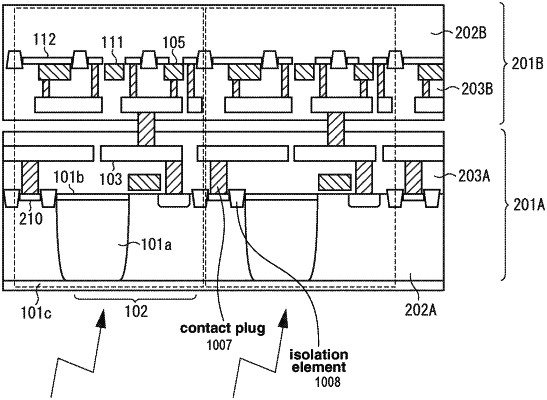
| CPC H01L 27/14623 (2013.01) [H01L 27/14607 (2013.01); H01L 27/1463 (2013.01); H01L 27/14634 (2013.01); H01L 27/1464 (2013.01); H01L 27/14641 (2013.01); H01L 27/148 (2013.01); H04N 25/59 (2023.01); H04N 25/71 (2023.01); H04N 25/75 (2023.01); H04N 25/771 (2023.01); H04N 25/772 (2023.01); H01L 27/14643 (2013.01)] | 32 Claims |

|
1. An imaging device comprising:
a first substrate;
a second substrate;
a plurality of photoelectric conversion units disposed in the first substrate within an area; and
a memory configured to hold a digital signal having a signal value corresponding to a signal generated by at least one of the plurality of photoelectric conversion units,
wherein a first light shielding member is disposed between the first substrate and the second substrate,
wherein at least a part of the memory is located within a first projection region defined by vertically projecting the first shielding member onto the second substrate side, and
wherein a second projection region defined by vertically projecting at least a part of the area onto the second substrate side, overlaps with the first projection region.
|