| CPC H01L 27/14621 (2013.01) [H01L 27/14601 (2013.01); H01L 27/1461 (2013.01); H01L 27/14629 (2013.01); H01L 27/1463 (2013.01)] | 4 Claims |

|
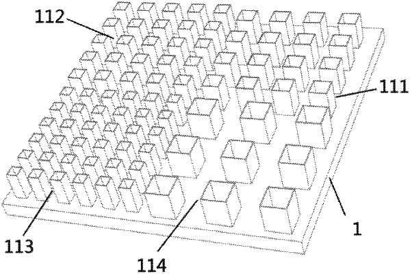
1. A wide spectral region multi-band detection structure with selective absorption enhancement is featured by comprising a plurality of sub-pixel units capable of detecting incident light in different bands, each sub-pixel unit is composed of a square well-shaped microstructure array and a metal lower electrode (2), a photosensitive layer (3), and an upper electrode (4) on the surface thereof, the size and array spacing of square well-shaped microstructures in different sub-pixel units are determined according to the detection bands of the sub-pixel units where they are located, the upper openings of the square well-shaped microstructures are hollow to form a resonant cavity, and the adjacent square well-shaped microstructures in the same sub-pixel unit form a resonant cavity;
further featured by comprising a substrate (1), which contains an array of red light square wells (101), green light square wells (102), blue light square wells (103) and near-infrared light square wells (104) on the upper-end face of the substrate, and contains the metal lower electrode (2), the photosensitive layer (3) and the upper electrode (4) on the structural surface of the substrate, the array structures of the red light square wells (101), the green light square wells (102), the blue light square wells (103) and the near-infrared light square wells (104) constitute a red light sub-pixel unit (111), a green light sub-pixel unit (112), a blue light sub-pixel unit (113) and a near-infrared light sub-pixel unit (114) together with the metal lower electrode (2), photosensitive layer (3) and the upper electrode (4) on their surfaces respectively, a filter is provided respectively above the red light sub-pixel unit (111), green light sub-pixel unit (112), blue light sub-pixel unit (113) and near-infrared light sub-pixel unit (114).
|